Features
● High efficiency
● High current capability
● High reliability
● High surge current capability
● Low power loss
● Glass passivated chip junction
● Solder dip 275 °C max. 7 s, per JESD 22-B106
1A1G
| VRRM (V) |
50 |
| lO (A) |
1 |
| IFSM (A) |
30 |
| VF (V) |
1.1 |
| IR(uA) @25℃ | 5 |
| Trr (ns) |
– |
| Tj (℃) |
-55~+125 |
| Package | T-1 |
Enquiry about 1A1G

Description
Typical Applications
Typical Applications
For use in general purpose rectification of power
supplies, inverters, converters, and freewheeling diodes for
consumer, and telecommunication
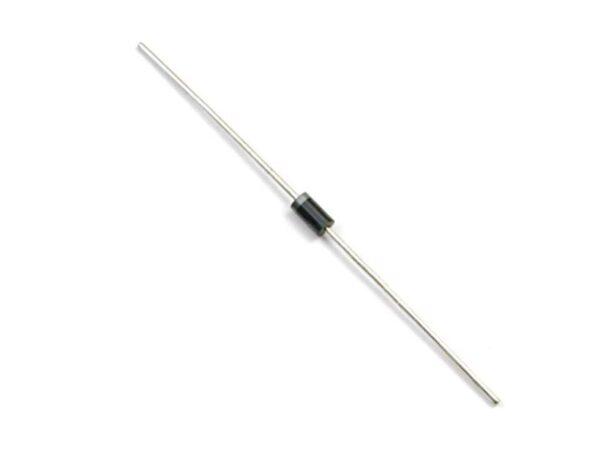
Mechanical Data
Mechanical Data
● Package:T-1
Molding compound meets UL 94 V-0 flammability rating,
RoHS-compliant
● Terminals: Tin plated leads, solderable per J-STD002 and JESD22-B102
● Polarity:Color band denotes cathode end
■ Maximum Ratings (Ta=25℃ Unless otherwise specified)
PARAMETER Symbol Unit 1A1G 1A2G 1A3G 1A4G 1A5G 1A6G 1A7G
Maximum Repetitive Peak Reverse Voltage VRRM V 50 100 200 400 600 800 1000
Maximum RMS Voltage VRMS V 35 70 140 280 420 560 700
Maximum DC blocking Voltage VDC V 50 100 200 400 600 800 1000
Average Forward Current
@Half-sine wave, Resistance load, Tc(Fig.1)
IO A 1.0
Forward Surge Current (Non-repetitive)
@60HZ sine wave, 1 cycle, Ta=25℃
IFSM A 30
Current squared time
@1ms≤t8.3≤ms Ta=25℃,Rating of per diode
I
2t A2s 3.7
Thermal Resistance(Typical)
@Between junction and case
RθJ-A ℃/W 65
Storage Temperature Tstg ℃ -55 ~ +150
Junction Temperature Tj ℃ -55 ~ +150
■ Electrical Characteristics(Ta=25℃ Unless otherwise specified)
PARAMETER Symbol Unit Conditions 1A1G 1A2G 1A3G 1A4G 1A5G 1A6G 1A7G
Peak Forward Voltage VFM V I F =1.0A 1.1
Peak Reverse Current IRRM μA
VR =VDC @Ta=25℃ 5
VR =VDC @Ta=125℃ 50
Datasheet